RF Solutions for harsh environments.
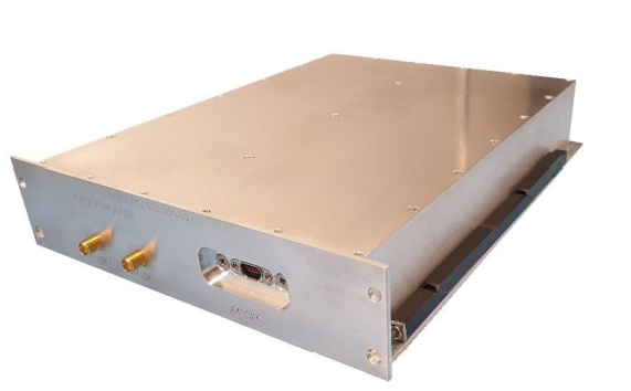
We are a specialist in the supply of custom microwave integrated modules for harsh environments. We operate to 100GHz and are active in Defence, Avionics, Marine, Satcom, medical and industrial markets.
Browse our products